- 您现在的位置:买卖IC网 > Sheet目录3882 > PIC16F77T-I/ML (Microchip Technology)IC MCU FLASH 8KX14 A/D 44QFN
PIC16F7X
DS30325B-page 32
2002 Microchip Technology Inc.
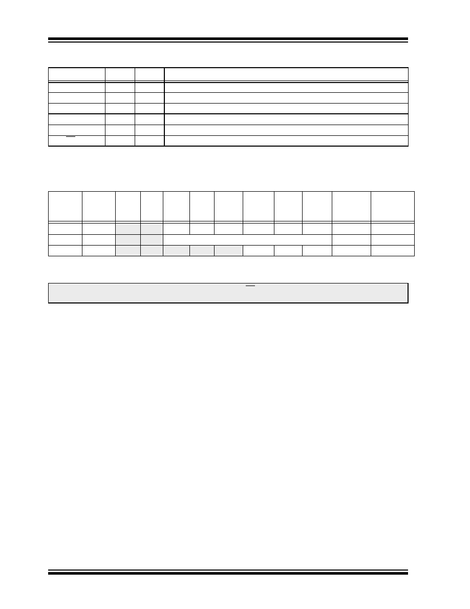
TABLE 4-1:
PORTA FUNCTIONS
TABLE 4-2:
SUMMARY OF REGISTERS ASSOCIATED WITH PORTA
Name
Bit#
Buffer
Function
RA0/AN0
bit0
TTL
Input/output or analog input.
RA1/AN1
bit1
TTL
Input/output or analog input.
RA2/AN2
bit2
TTL
Input/output or analog input.
RA3/AN3/VREF
bit3
TTL
Input/output or analog input or VREF.
RA4/T0CKI
bit4
ST
Input/output or external clock input for Timer0. Output is open drain type.
RA5/SS/AN4
bit5
TTL
Input/output or slave select input for synchronous serial port or analog input.
Legend: TTL = TTL input, ST = Schmitt Trigger input
Address
Name
Bit 7
Bit 6
Bit 5
Bit 4
Bit 3
Bit 2
Bit 1
Bit 0
Value on:
POR,
BOR
Value on all
other
RESETS
05h
PORTA
—
RA5
RA4
RA3
RA2
RA1
RA0
--0x 0000
--0u 0000
85h
TRISA
—
PORTA Data Direction Register
--11 1111
9Fh
ADCON1
—
PCFG2
PCFG1 PCFG0 ---- -000
---- -000
Legend: x = unknown, u = unchanged, - = unimplemented locations read as '0'. Shaded cells are not used by PORTA.
Note:
When using the SSP module in SPI Slave mode and SS enabled, the A/D converter must be set to one of
the following modes where PCFG2:PCFG0 = 100, 101, 11x.
发布紧急采购,3分钟左右您将得到回复。
相关PDF资料
PIC18F24K20-I/SS
IC PIC MCU FLASH 8KX16 28SSOP
PIC16F77-E/ML
IC MCU FLASH 8KX14 A/D 44QFN
PIC16LF74T-I/ML
IC MCU FLASH 4KX14 A/D 44QFN
PIC16F723-I/MV
IC MCU 8BIT 7KB FLASH 28UQFN
PIC18F442T-I/ML
IC MCU FLASH 8KX16 EE A/D 44QFN
PIC18LF2439-I/SP
IC MCU FLASH 6KX16 EE A/D 28DIP
PIC16F687-I/ML
IC PIC MCU FLASH 2KX14 20QFN
PIC18LF2439-I/SO
IC MCU FLASH 6KX16 EE A/D 28SOIC
相关代理商/技术参数
PIC16F77T-I/PT
功能描述:8位微控制器 -MCU 14KB 368 RAM 33 I/O RoHS:否 制造商:Silicon Labs 核心:8051 处理器系列:C8051F39x 数据总线宽度:8 bit 最大时钟频率:50 MHz 程序存储器大小:16 KB 数据 RAM 大小:1 KB 片上 ADC:Yes 工作电源电压:1.8 V to 3.6 V 工作温度范围:- 40 C to + 105 C 封装 / 箱体:QFN-20 安装风格:SMD/SMT
PIC16F77T-I/PTG
功能描述:8位微控制器 -MCU 14KB 368 RAM 33 I/O RoHS:否 制造商:Silicon Labs 核心:8051 处理器系列:C8051F39x 数据总线宽度:8 bit 最大时钟频率:50 MHz 程序存储器大小:16 KB 数据 RAM 大小:1 KB 片上 ADC:Yes 工作电源电压:1.8 V to 3.6 V 工作温度范围:- 40 C to + 105 C 封装 / 箱体:QFN-20 安装风格:SMD/SMT
PIC16F77TIPT
制造商:MICROCHIP 功能描述:New
PIC16F785-E/ML
功能描述:8位微控制器 -MCU 3.5 KB 128 RAM 18I/O RoHS:否 制造商:Silicon Labs 核心:8051 处理器系列:C8051F39x 数据总线宽度:8 bit 最大时钟频率:50 MHz 程序存储器大小:16 KB 数据 RAM 大小:1 KB 片上 ADC:Yes 工作电源电压:1.8 V to 3.6 V 工作温度范围:- 40 C to + 105 C 封装 / 箱体:QFN-20 安装风格:SMD/SMT
PIC16F785-E/P
功能描述:8位微控制器 -MCU 14KB 368 RAM 33 I/O RoHS:否 制造商:Silicon Labs 核心:8051 处理器系列:C8051F39x 数据总线宽度:8 bit 最大时钟频率:50 MHz 程序存储器大小:16 KB 数据 RAM 大小:1 KB 片上 ADC:Yes 工作电源电压:1.8 V to 3.6 V 工作温度范围:- 40 C to + 105 C 封装 / 箱体:QFN-20 安装风格:SMD/SMT
PIC16F785-E/SO
功能描述:8位微控制器 -MCU 3.5KB FL 128R 18 I/O RoHS:否 制造商:Silicon Labs 核心:8051 处理器系列:C8051F39x 数据总线宽度:8 bit 最大时钟频率:50 MHz 程序存储器大小:16 KB 数据 RAM 大小:1 KB 片上 ADC:Yes 工作电源电压:1.8 V to 3.6 V 工作温度范围:- 40 C to + 105 C 封装 / 箱体:QFN-20 安装风格:SMD/SMT
PIC16F785-E/SS
功能描述:8位微控制器 -MCU 3.5KB FL 128R 18 I/O RoHS:否 制造商:Silicon Labs 核心:8051 处理器系列:C8051F39x 数据总线宽度:8 bit 最大时钟频率:50 MHz 程序存储器大小:16 KB 数据 RAM 大小:1 KB 片上 ADC:Yes 工作电源电压:1.8 V to 3.6 V 工作温度范围:- 40 C to + 105 C 封装 / 箱体:QFN-20 安装风格:SMD/SMT
PIC16F785-I/ML
功能描述:8位微控制器 -MCU 3.5 KB 128 RAM 18I/O RoHS:否 制造商:Silicon Labs 核心:8051 处理器系列:C8051F39x 数据总线宽度:8 bit 最大时钟频率:50 MHz 程序存储器大小:16 KB 数据 RAM 大小:1 KB 片上 ADC:Yes 工作电源电压:1.8 V to 3.6 V 工作温度范围:- 40 C to + 105 C 封装 / 箱体:QFN-20 安装风格:SMD/SMT